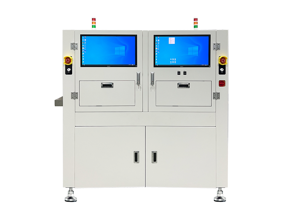

Precision RF & Ferrite Inductor Optical Inspection
The high-end visual inspection equipment based on vector algorithm and AI visual inspection technology solves the quality problems of semiconductor chips due to the limitations of production and process skills.
◆ The key parameters
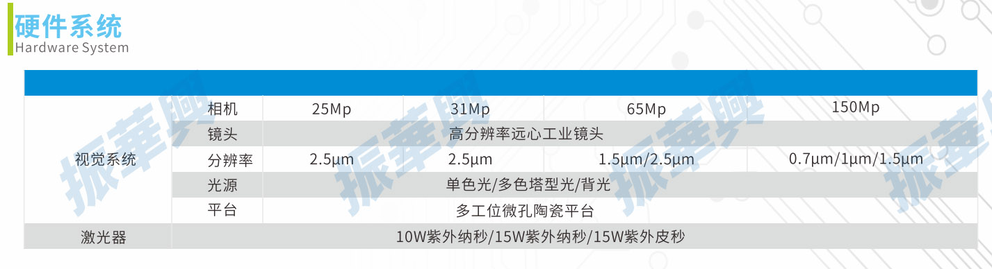
● Standard 2.5μm high resolution image precision detection, optional higher resolution
● 25 megapixel industrial camera with 31 megapixel, 65 megapixel, 150 megapixel options
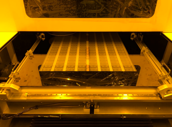
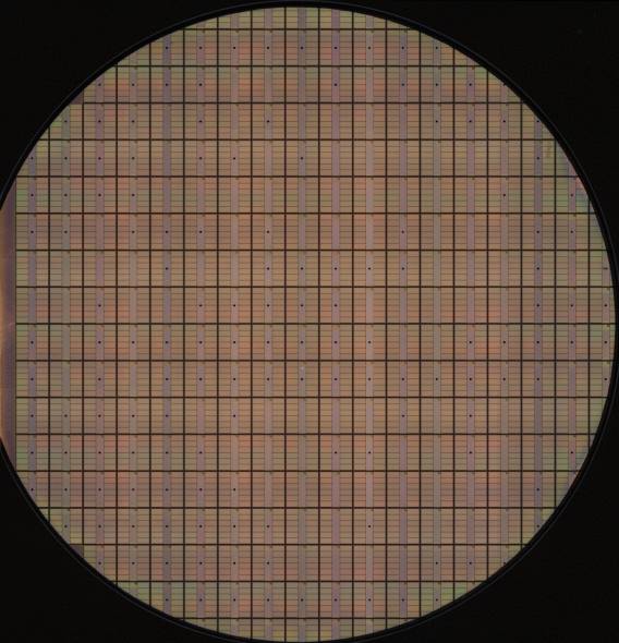
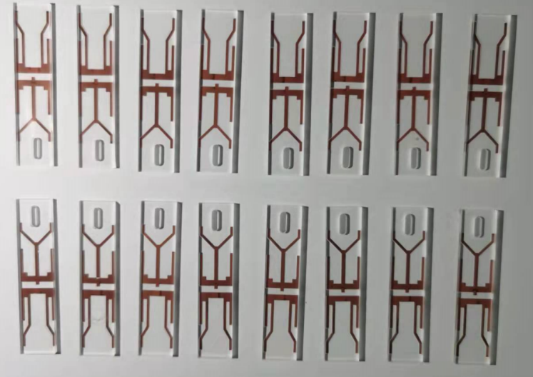
● Can detect LTCC, ferrite, high-frequency laminated ceramic inductor, wafer class, SIP packaging class and other semiconductor materials appearance detection
● Visual inspection system supports offline programming, online debugging, AI intelligent review
●NG/OK automatic sorting, automatic laser pick waste

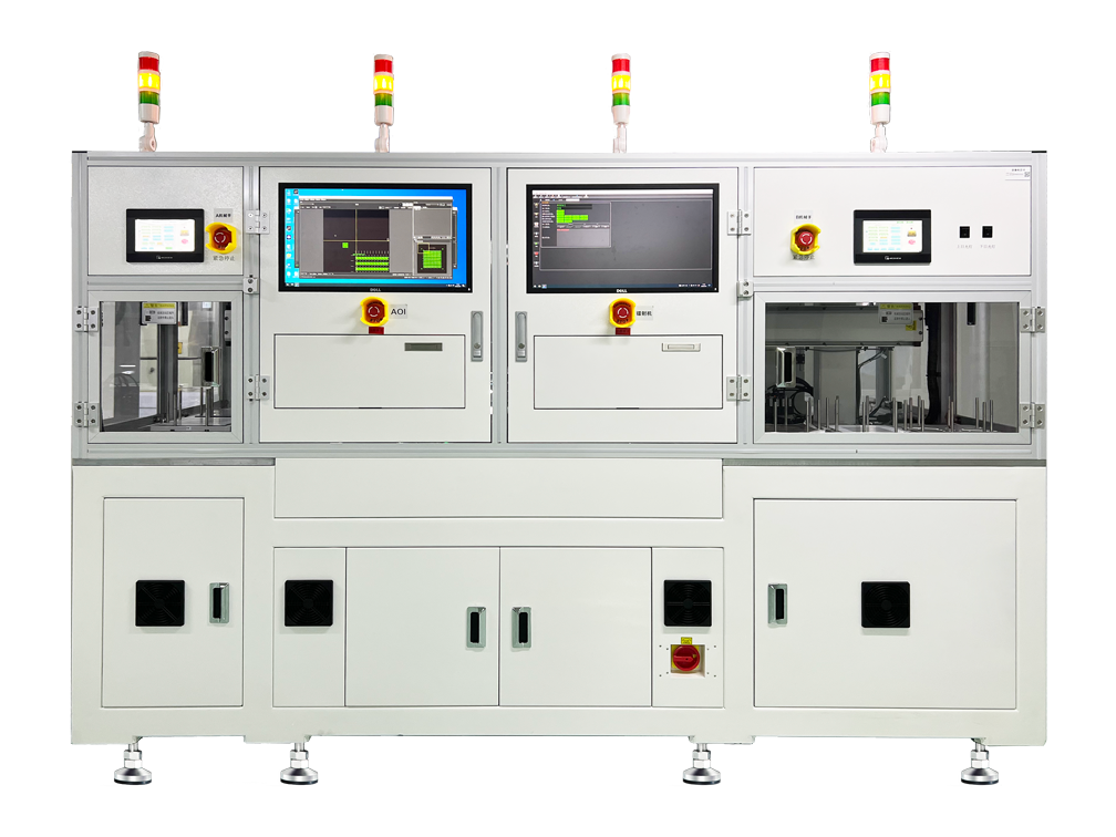
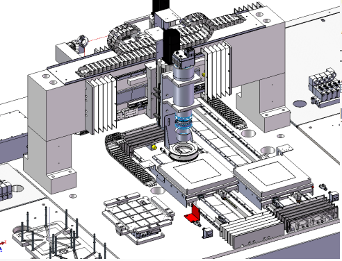
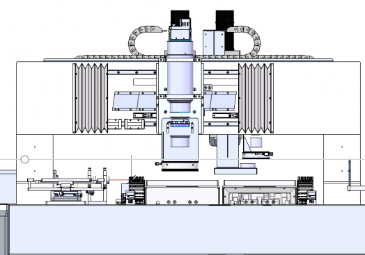
◆ AOI inspection
● Marble gantry structure design, configuration of high precision linear electrical module,
to ensure X,Y axis operation accuracy, the highest accuracy of ±1μm
●25 megapixel industrial camera, high resolution telecentric lens, 0.2~2.5μm/pixel high
resolution optional
● Single material slice detection CT < 30 seconds @200*200mm, CCD height can automatically
adjust the range of ±5mm
● can detect the effective area of 50*50~400*300mm, and output OK, NG, TBC (beyond a certain
proportion of the set number of bad value for the confirmation area,
The product will be grabbed by the manipulator and placed in the radium cutting module to
perform radium cutting)
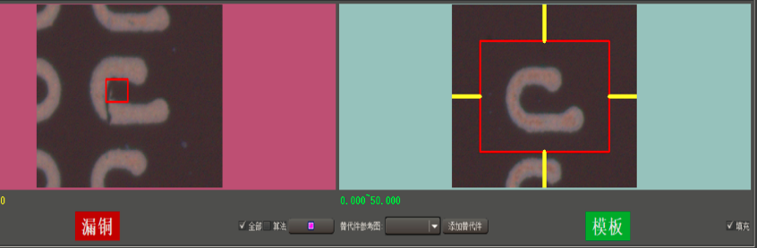
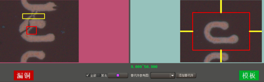
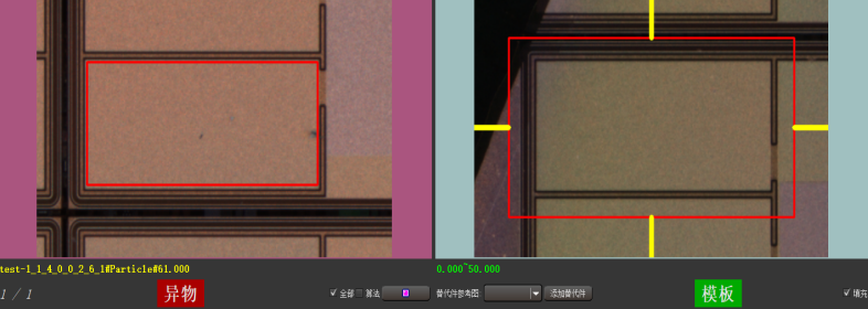
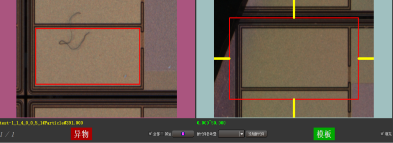
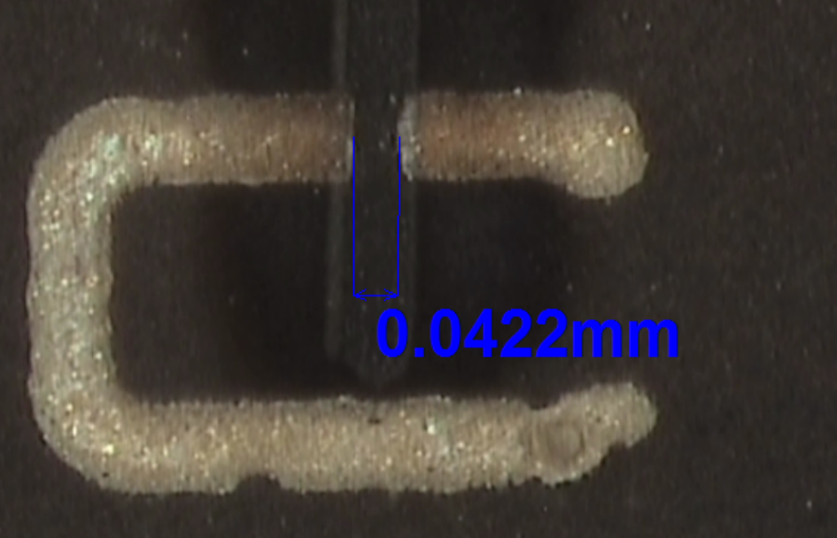
● Can detect all kinds of appearance defects such as broken thread, burr, pinhole, foreign body,
notch, length, width, area, abnormity, etc
◆ Software algorithm
● Independent intellectual property rights of the optical detection software system,
based on vector analysis algorithm rules, integration of logic or operation, brightness
range, brightness change minimum span
Degree, AI deep learning and more than 30 advanced detection algorithms, to deal
with a variety of complex lines and semiconductor parts detection
● Support SPC statistical analysis function, support various production intelligent
execution system SFC/MES docking
● Support AI intelligent reply function
● Support offline programming & online non-stop debugging function

◆ Detect bad components
◆ The laser cutting
● Image recognition system to detect the completion of the product automatic
execution judgment:
● Test the product without defect by the material module automatically grab the
product to the OK material box
● Test beyond the number of defects or a certain percentage of products by the
cutting module will automatically grab the product to the NG box
● If the number or percentage of test defects is within the control range, the cutting
module will automatically capture the product to the radium cutting area and perform
automatic radium cutting
◆ Application Area

|
|
| Wafer | SIP Encapsulation |
Consumer protection service items usually include "free warranty maintenance",
"regular return visit", "on-site training", "24-hour appeal response" and other
categories. We provide customers with the best equipment and perfect fast
service guarantee with the most sincere attitude.
● The equipment shall be guaranteed free of charge for one year and maintained
for life from the date of acceptance. The operationcontrol software of the sold
equipment shall be upgraded free of charge for life to ensure the latest software
version and optimization of functions.
● Call back and visit customers irregularly, communicate with customers in time
and improve relevant problems.
● The Customer Service Department shall respond to customer demands within
24 hours and within 2 hours after receiving them.
Overseas customers can provide nearby technical services or provide remote
training and technical support according to actual needs.

Customer-centric, quality as life
Taking innovation as the driving force and
talent as the foundation